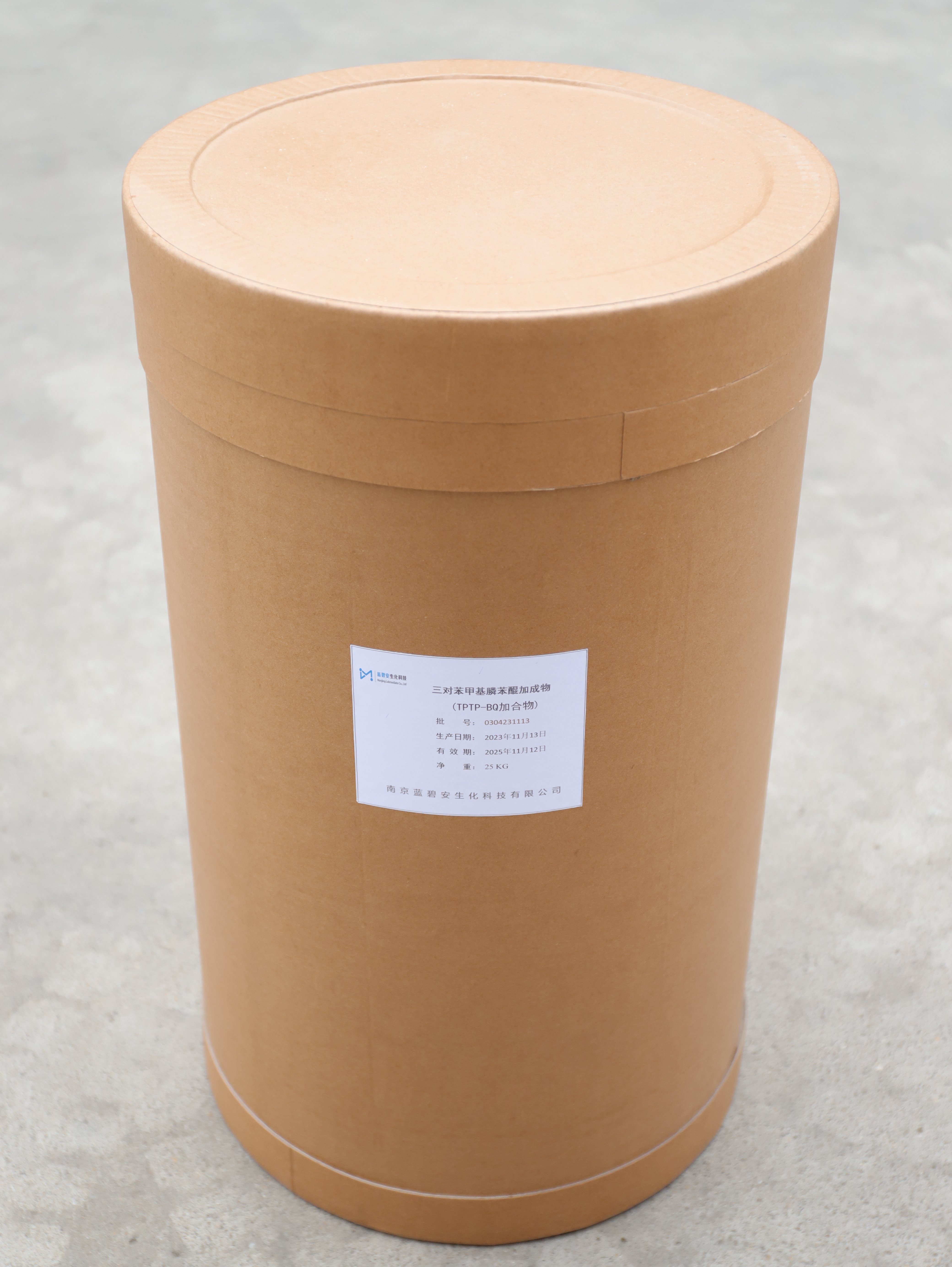
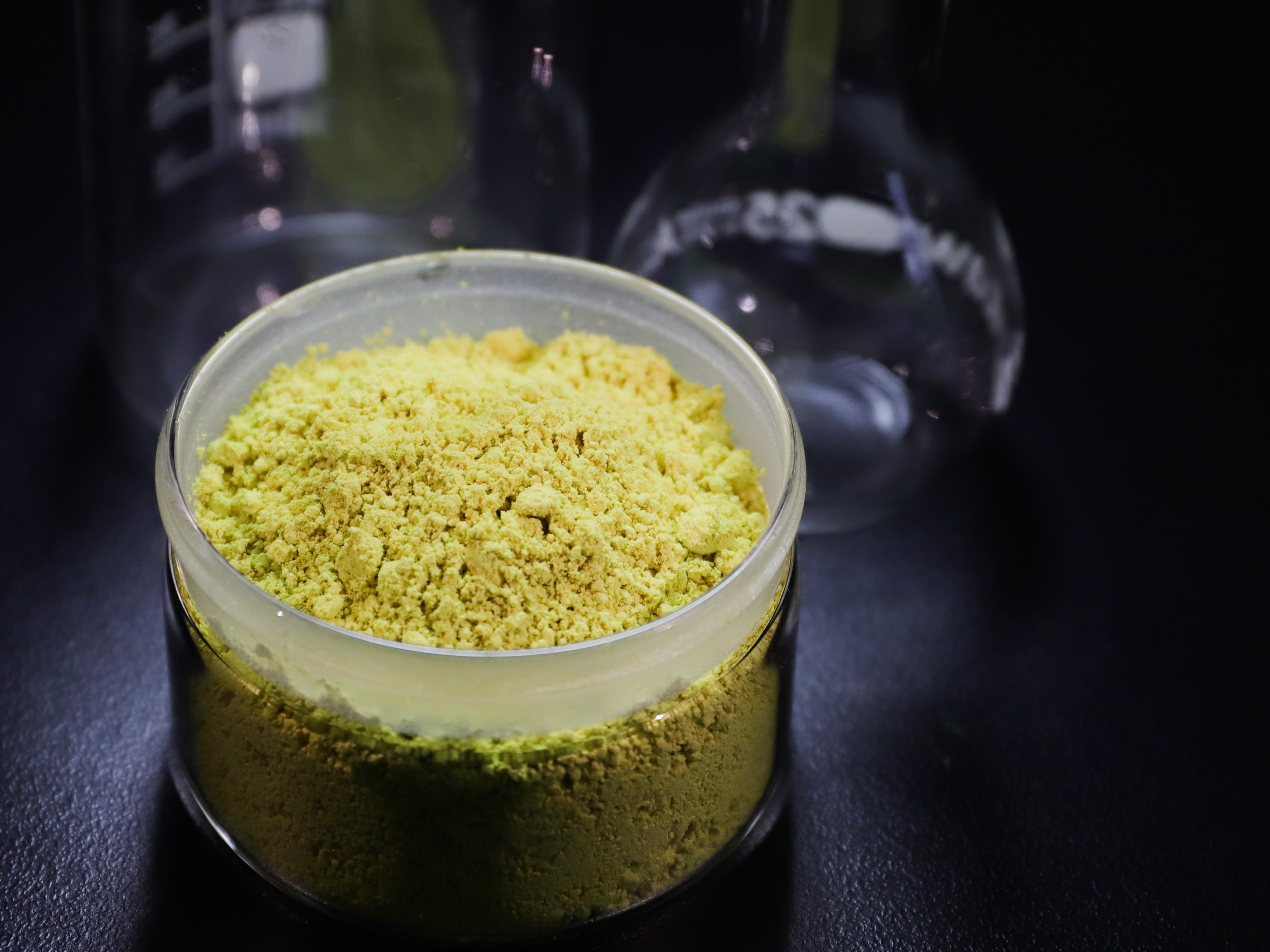
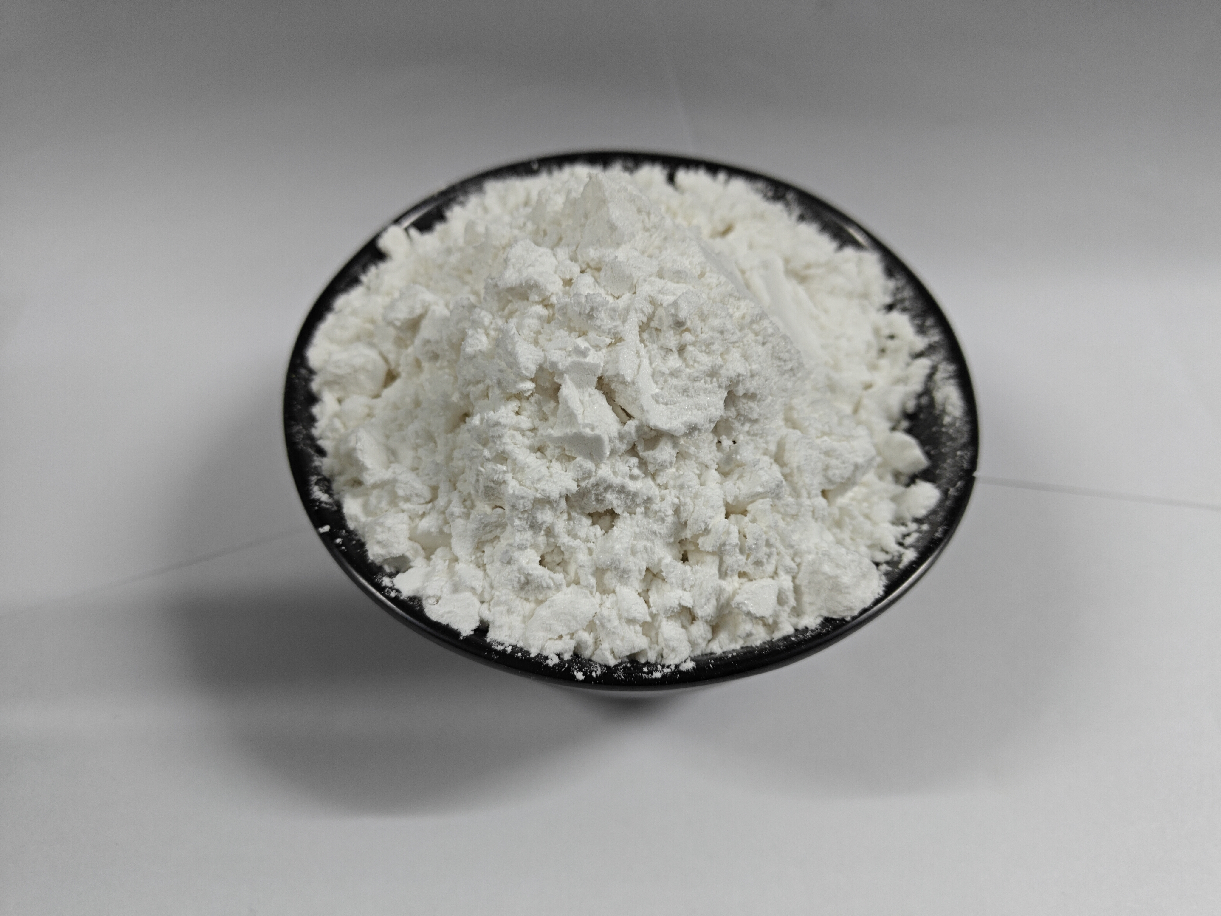
Semiconductor Encapsulant Curing Agent Solutions

All Categories

semiconductor encapsulant curing agent

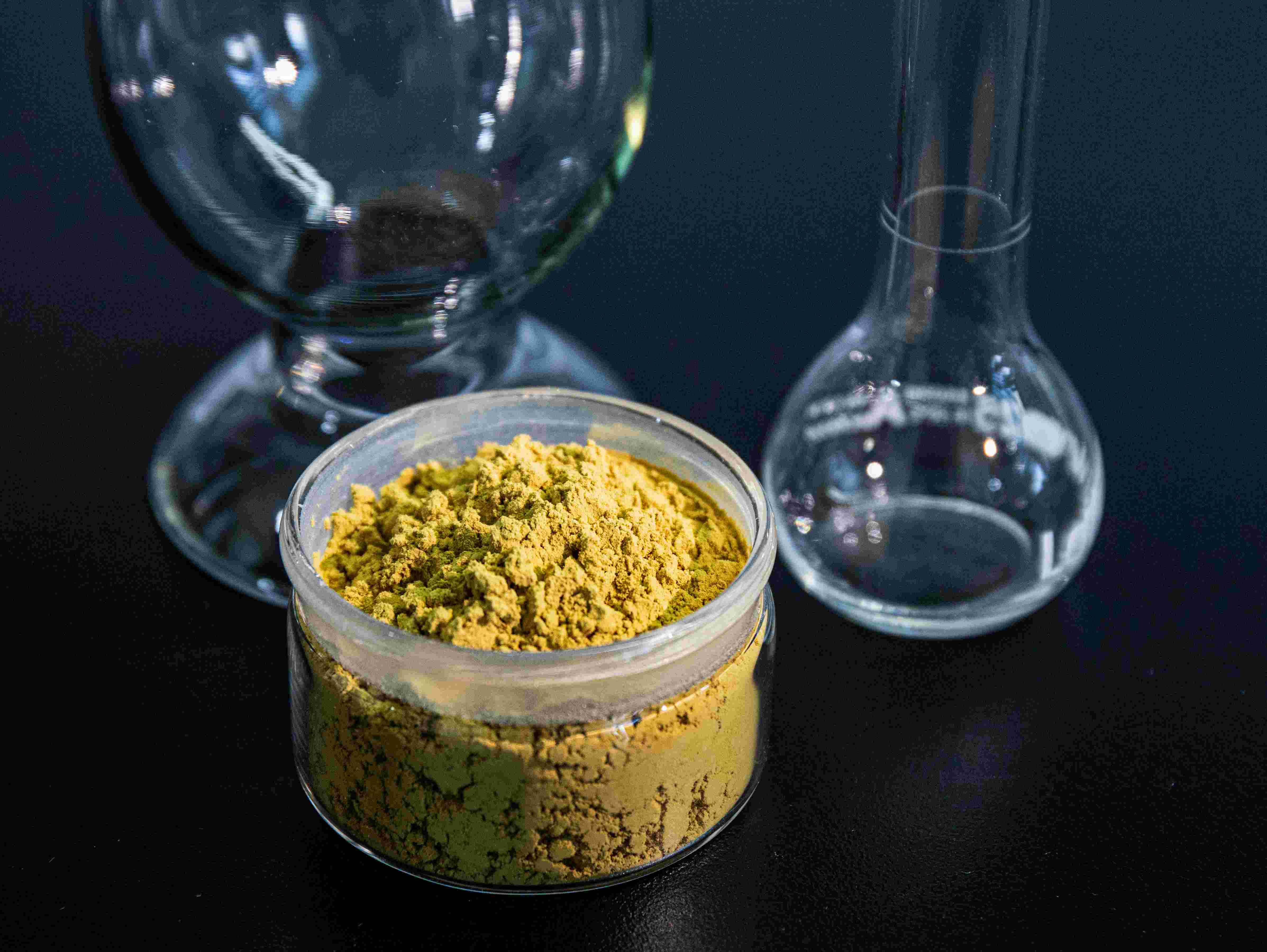
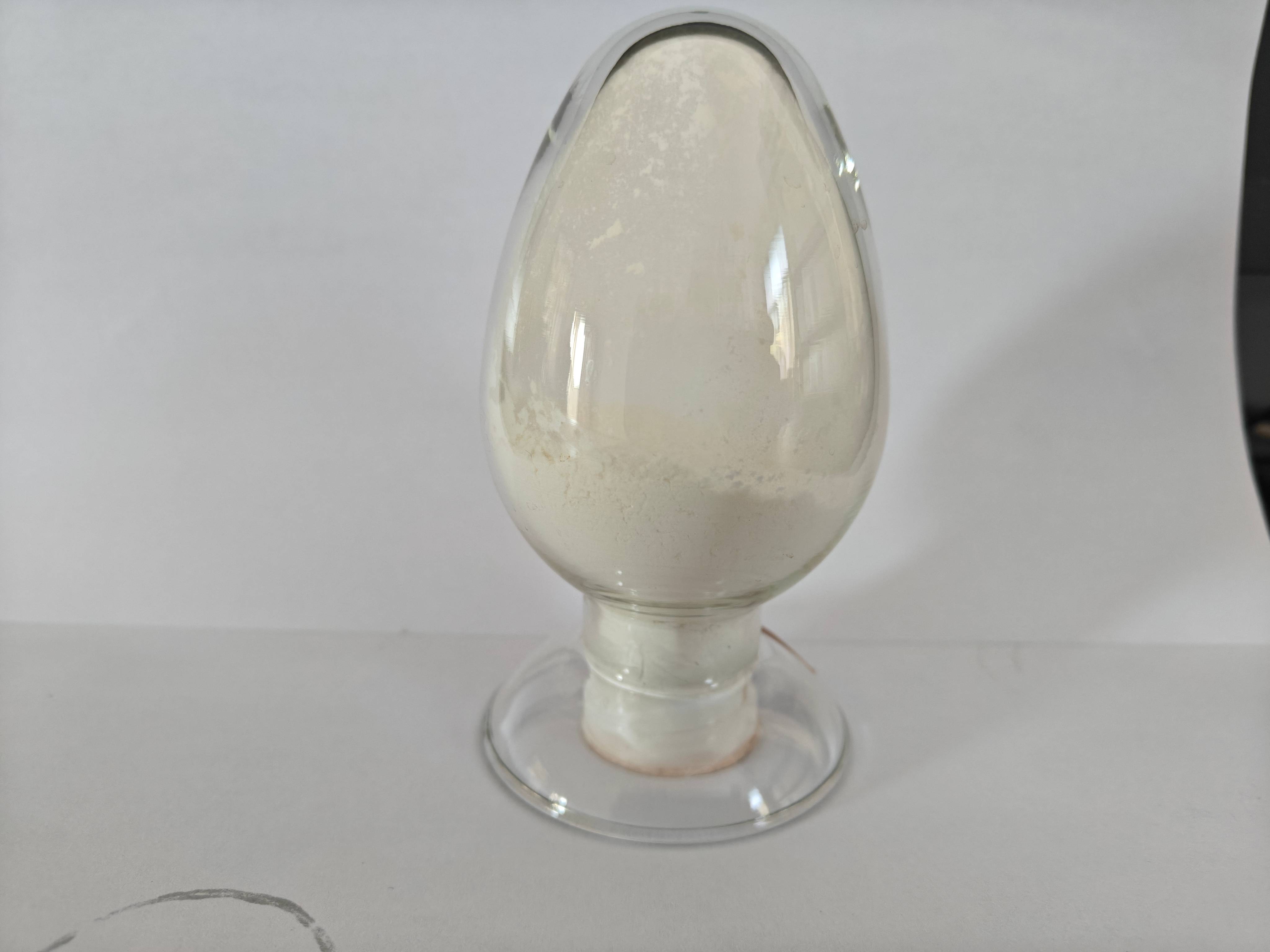
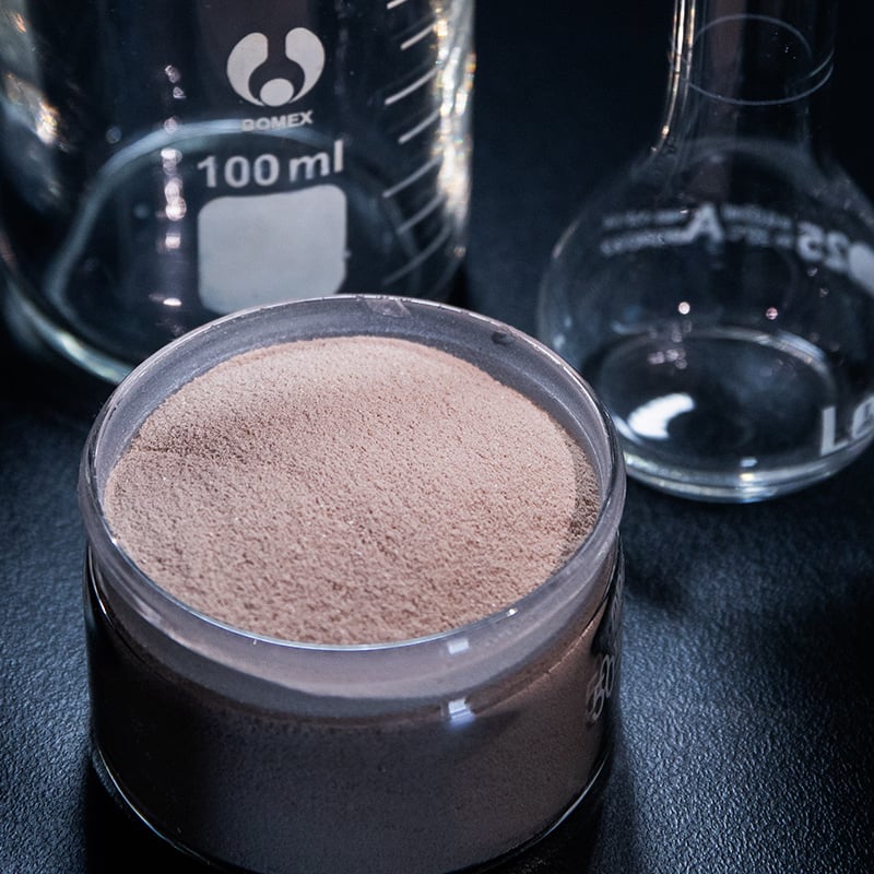
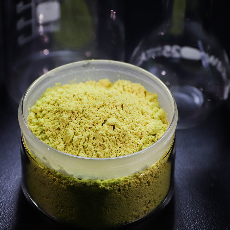
A semiconductor encapsulant curing agent is a specialized chemical compound that initiates and controls the hardening process of epoxy resins used in electronic component packaging. This critical material transforms liquid encapsulant formulations into solid protective layers that shield semiconductor devices from environmental stress, moisture, and mechanical damage. The semiconductor encapsulant curing agent works by triggering cross-linking reactions within the resin matrix, creating a durable three-dimensional polymer network. Modern formulations are engineered to provide precise control over curing temperature, reaction speed, and final material properties. These agents typically consist of anhydrides, phenolic compounds, or amine-based systems selected based on specific application requirements. The technology enables manufacturers to achieve optimal balance between processing efficiency and product reliability. Key functions include accelerating polymerization reactions, reducing cure times, improving adhesion to substrate materials, and enhancing thermal stability of the final encapsulation. The semiconductor encapsulant curing agent must maintain consistent performance across varying production conditions while ensuring compatibility with sensitive electronic components. Advanced formulations deliver low-stress curing profiles that prevent warpage and cracking in delicate semiconductor structures. These agents also influence critical properties such as glass transition temperature, coefficient of thermal expansion, and moisture absorption rates. The selection of appropriate curing agent chemistry directly impacts production throughput, energy consumption, and long-term device reliability, making it an essential consideration in semiconductor manufacturing processes.
New Products

Choosing the right semiconductor encapsulant curing agent delivers substantial benefits that directly impact your production efficiency and product quality. First, these specialized agents significantly reduce manufacturing cycle times by enabling faster curing at lower temperatures, which translates to increased throughput and reduced energy costs in your facility. You can process more units per hour while consuming less power, directly improving your bottom line. The controlled reaction kinetics prevent premature gelation during mixing and application stages, giving your operators a comfortable working window to ensure proper component coverage. This operational flexibility reduces material waste and rework costs. When properly formulated, a semiconductor encapsulant curing agent enhances the mechanical strength and chemical resistance of the final package, providing superior protection against harsh operating environments. Your products gain extended service life and improved reliability ratings, which strengthen customer satisfaction and reduce warranty claims. The low-stress curing mechanism minimizes internal tensions within the package structure, preventing delamination and cracking issues that compromise device performance. This becomes especially valuable when working with thin dies and advanced packaging configurations where mechanical stress can cause immediate or latent failures. Additionally, modern curing agents offer excellent compatibility with various filler systems and additives, allowing you to customize formulations for specific thermal conductivity, flame retardancy, or electrical insulation requirements. The chemical stability of these agents ensures consistent batch-to-batch performance, eliminating production variability that leads to quality control headaches. By optimizing cure profiles, you can also reduce post-cure requirements, further streamlining your manufacturing workflow and accelerating time-to-market for new product introductions.

Tips And Tricks

What Should Manufacturers Look for When Choosing Thermally Latent Catalysts?

12

Dec

What Should Manufacturers Look for When Choosing Thermally Latent Catalysts?

Manufacturing processes across industries rely heavily on precise chemical reactions, and selecting the right thermally latent catalysts can determine the success or failure of production outcomes. These specialized catalytic compounds remain inactiv...
View More
How do procurement teams compare CDI coupling reagent suppliers

07

Jan

How do procurement teams compare CDI coupling reagent suppliers

Procurement teams in pharmaceutical and biotechnology companies face a complex decision when selecting suppliers for specialized chemical reagents. The evaluation of cdi coupling reagent suppliers requires a comprehensive understanding of product spe...
View More
How do manufacturers optimize CDI amide bonds for production use

07

Jan

How do manufacturers optimize CDI amide bonds for production use

Chemical manufacturing processes rely heavily on efficient bond formation techniques to create stable molecular structures for various industrial applications. Among the most significant developments in organic synthesis, cdi amide bonds represent a ...
View More
Which Factors Affect the Efficiency of Curing Agents in Epoxy Resin Systems?

12

Feb

Which Factors Affect the Efficiency of Curing Agents in Epoxy Resin Systems?

The efficiency of curing agents in epoxy resin systems depends on numerous interconnected factors that directly influence the polymerization process and final material properties. Understanding these variables is crucial for optimizing epoxy formulat...
View More

Get a Free Quote

Our representative will contact you soon.
Email
Name
Company Name
Message
0/1000

semiconductor encapsulant curing agent

Optimized Thermal Performance and Dimensional Stability

Optimized Thermal Performance and Dimensional Stability

The semiconductor encapsulant curing agent plays a pivotal role in achieving superior thermal management and dimensional stability throughout the device lifecycle. Advanced curing chemistry creates polymer networks with precisely controlled cross-link density, resulting in optimal glass transition temperatures that maintain structural integrity across extreme temperature fluctuations. This thermal stability prevents package deformation during assembly processes like solder reflow and wire bonding, where temperatures often exceed 250 degrees Celsius. The carefully engineered coefficient of thermal expansion matching between the cured encapsulant and substrate materials minimizes interfacial stress accumulation during thermal cycling. This stress reduction is critical for preventing fatigue-induced failures in solder joints and interconnects. Furthermore, the curing agent influences the thermal conductivity of the final compound by facilitating uniform filler dispersion and strong interfacial bonding. Enhanced heat dissipation capability protects sensitive semiconductor junctions from thermal runaway conditions, extending device operational life. The low-shrinkage characteristics during polymerization ensure accurate dimensional control, maintaining tight tolerances required for modern high-density packaging architectures. These combined thermal and mechanical properties deliver robust protection that meets stringent reliability standards for automotive, aerospace, and industrial electronics applications.
Extended Pot Life with Rapid On-Demand Curing

Extended Pot Life with Rapid On-Demand Curing

Modern semiconductor encapsulant curing agent formulations solve the traditional trade-off between working time and production speed through innovative latent catalyst technology. These intelligent systems remain chemically dormant at room temperature, providing extended pot life that can span several hours or even days, depending on the specific chemistry selected. This extended usability window eliminates the pressure of rushed application and reduces material waste from premature gelation in mixing equipment and dispensing systems. Operators gain the flexibility to prepare larger batches, reducing setup frequency and improving material utilization rates. However, when heat is applied, the semiconductor encapsulant curing agent activates rapidly, initiating fast polymerization that completes the curing cycle in minutes rather than hours. This on-demand activation provides manufacturers with the best of both worlds: convenience during handling and speed during production. The sharp activation profile also enables precise process control through temperature management, allowing fine-tuning of cure schedules to match specific production requirements. This responsiveness supports lean manufacturing principles by minimizing work-in-process inventory and reducing floor space dedicated to curing operations. The predictable activation behavior ensures consistent quality across production runs, supporting statistical process control initiatives and facilitating compliance with industry quality standards.
Enhanced Compatibility with Advanced Packaging Technologies

Enhanced Compatibility with Advanced Packaging Technologies

As semiconductor packaging evolves toward increasingly complex three-dimensional architectures and heterogeneous integration approaches, the semiconductor encapsulant curing agent must meet demanding compatibility requirements. Contemporary formulations are specifically designed to work seamlessly with low-k dielectrics, copper pillar bumps, through-silicon vias, and other advanced interconnect technologies without causing corrosion, delamination, or electrical performance degradation. The carefully controlled ionic content and chemical purity prevent contamination that could compromise device reliability or introduce unwanted leakage currents. These agents demonstrate excellent adhesion to diverse substrate materials including organic laminates, ceramic carriers, glass interposers, and metal heat spreaders, ensuring robust mechanical attachment across multi-material interfaces. The low-outgassing characteristics prevent void formation and maintain optical clarity requirements for optoelectronic applications. Additionally, the semiconductor encapsulant curing agent supports ultra-thin encapsulation profiles required for stacked die configurations and wafer-level packaging approaches, where traditional thick encapsulation methods prove impractical. The fine-tuned rheology control during the early cure stages enables complete penetration into narrow gaps and underfill regions, eliminating voids that create stress concentration points. This comprehensive compatibility ensures that manufacturers can adopt next-generation packaging innovations without reformulating their entire material systems, protecting existing process investments while enabling technology advancement.

Get a Free Quote

Our representative will contact you soon.
Email
Name
Company Name
Message
0/1000