Semiconductor Encapsulant Hardener Solutions

All Categories

semiconductor encapsulant hardener

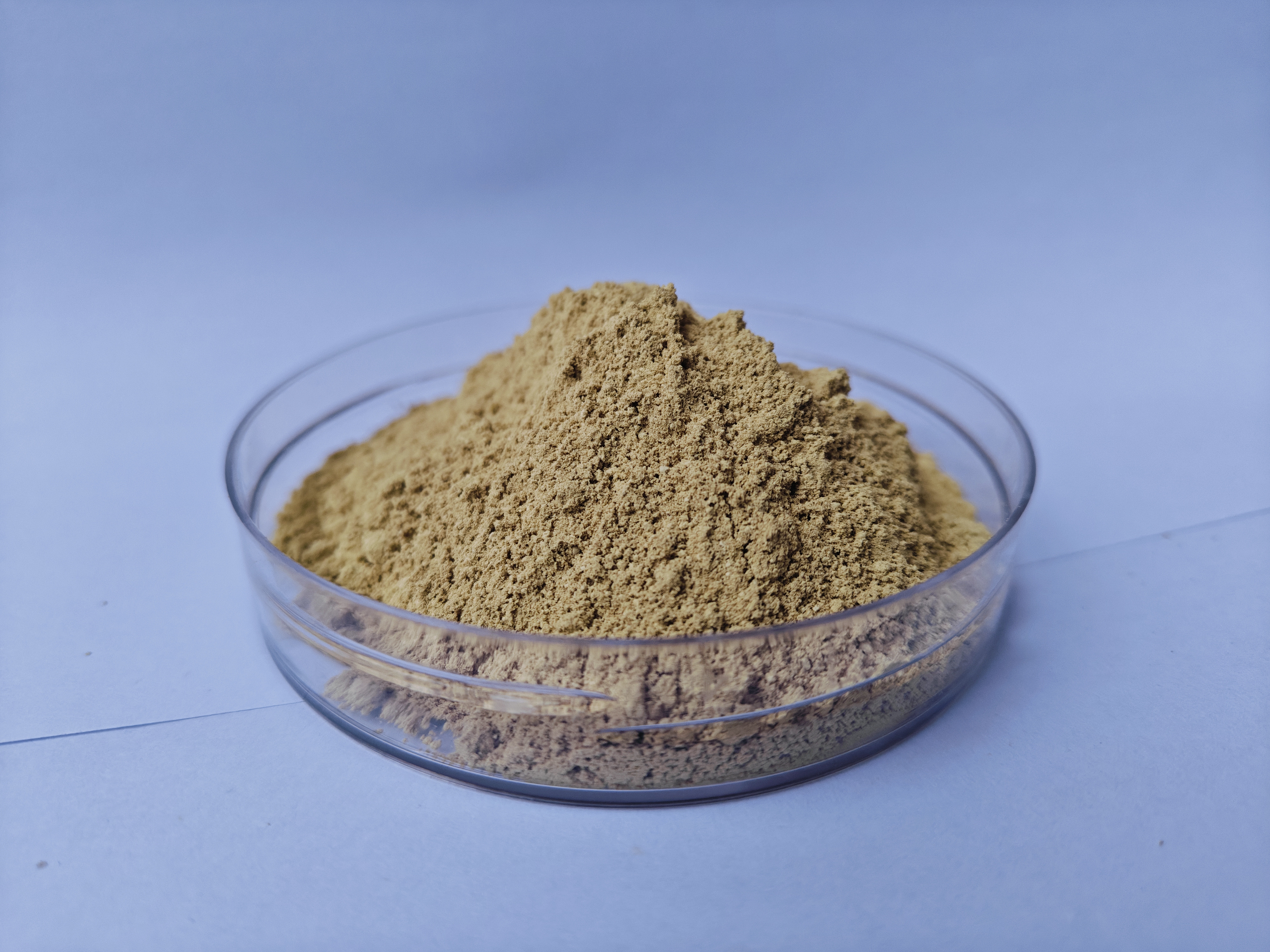
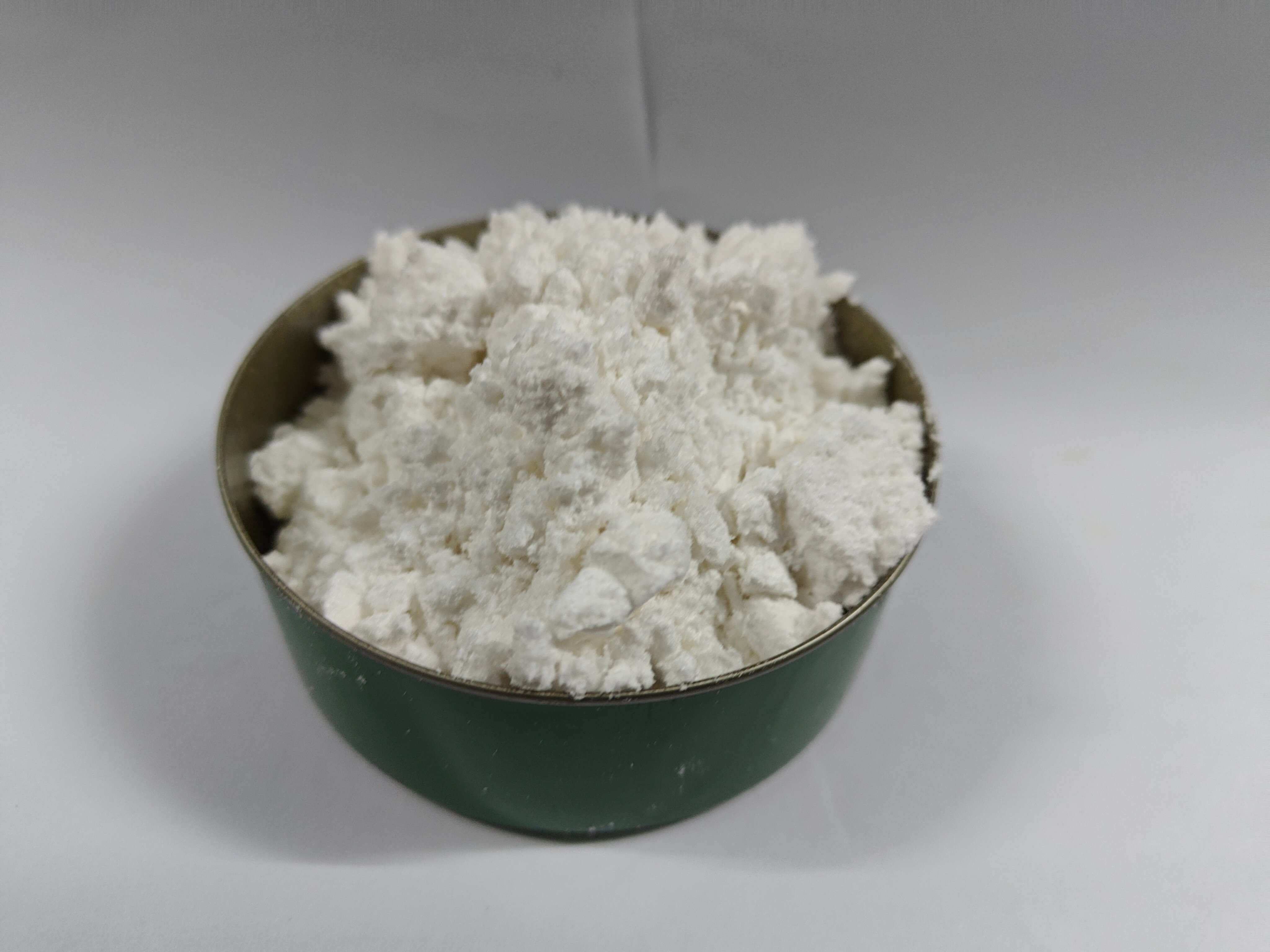
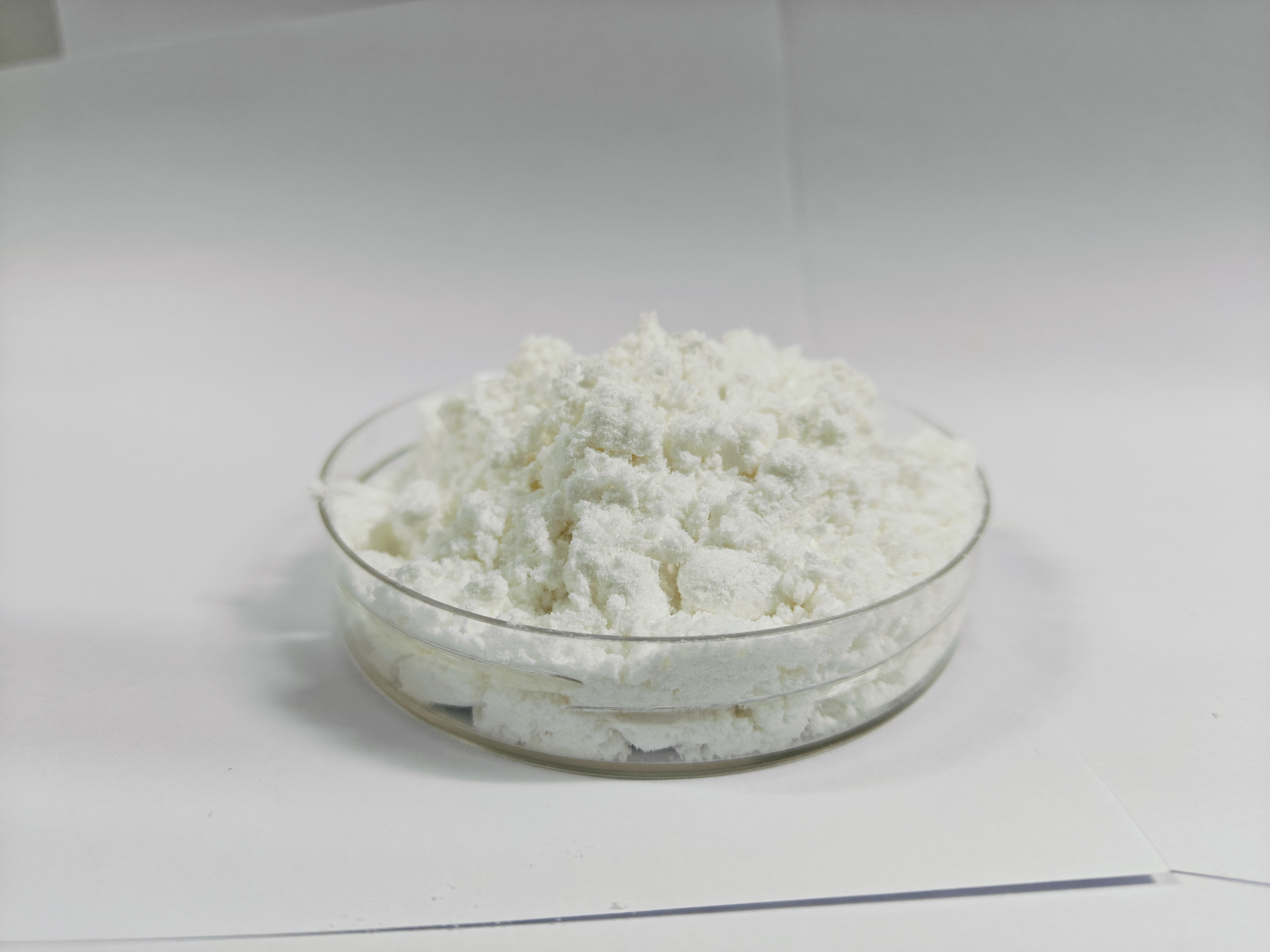
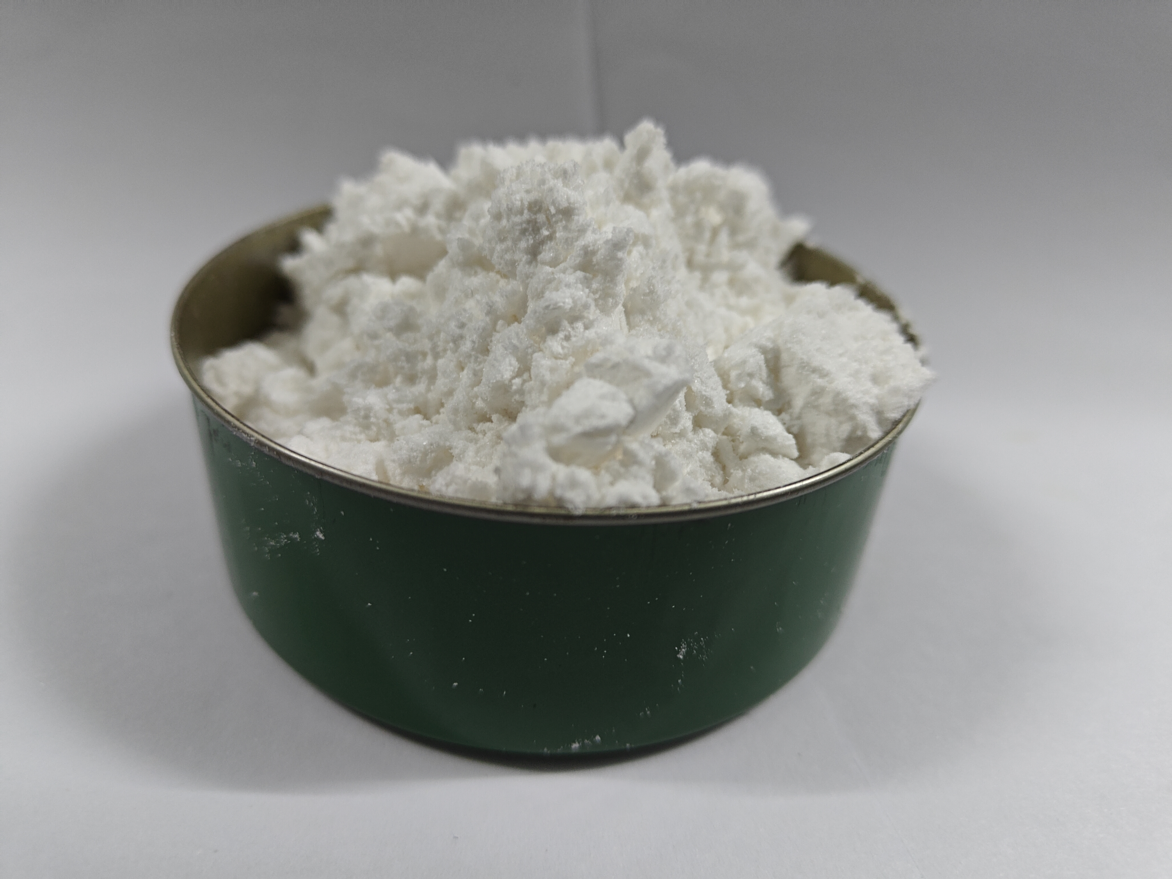
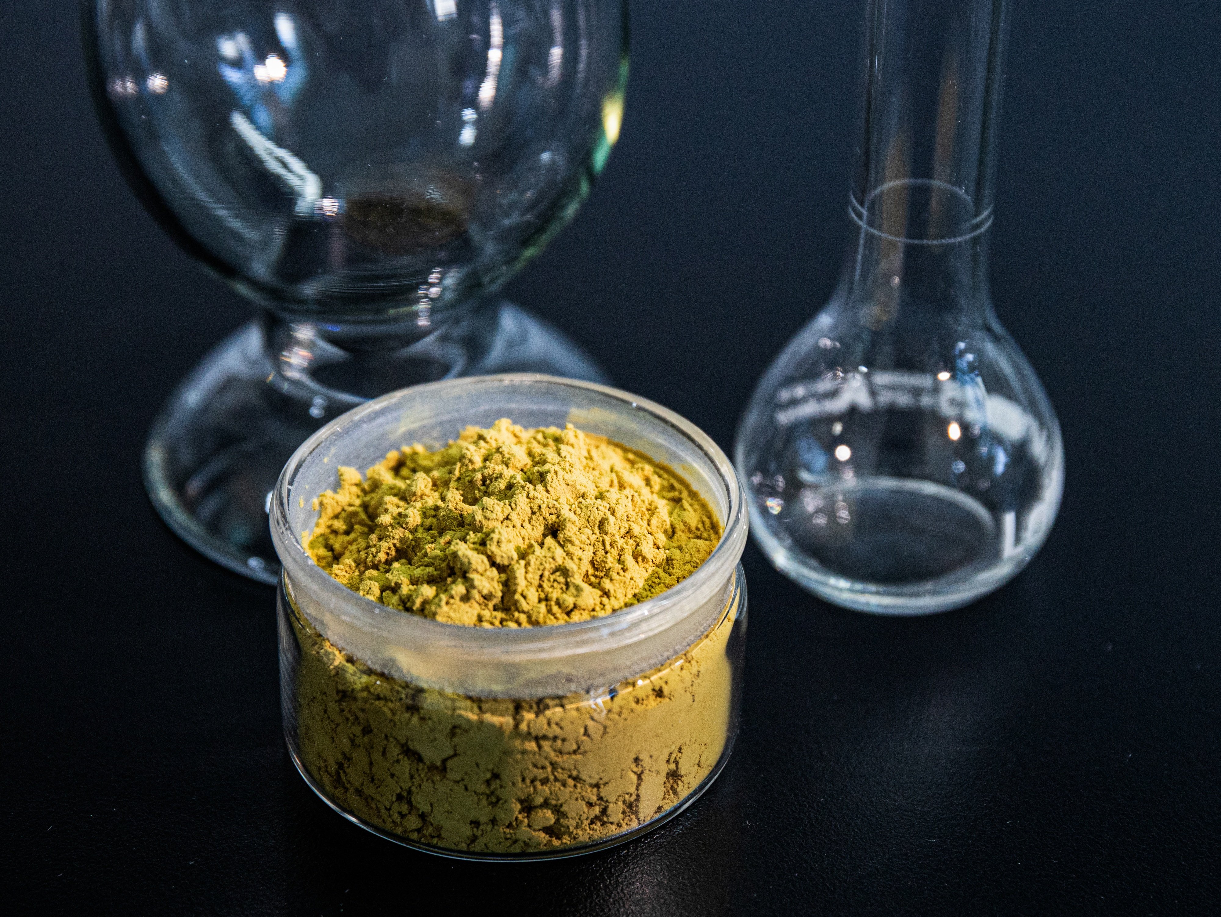
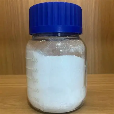
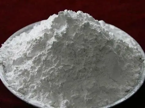
A semiconductor encapsulant hardener is a critical chemical component used in the electronic packaging industry to cure and solidify epoxy resin formulations that protect semiconductor devices. This specialized hardening agent works by initiating a cross-linking reaction when mixed with epoxy resins, transforming liquid encapsulant materials into durable, protective solid coatings. The semiconductor encapsulant hardener plays an essential role in ensuring the reliability and longevity of microchips, integrated circuits, and other electronic components by providing superior mechanical strength, thermal stability, and chemical resistance. These hardeners are specifically formulated to meet the demanding requirements of semiconductor manufacturing, where precision and consistency are paramount. The curing process facilitated by the semiconductor encapsulant hardener creates a robust protective barrier that shields delicate semiconductor structures from moisture, contaminants, thermal stress, and mechanical damage. Modern formulations are designed to offer controlled curing speeds, low shrinkage rates, and excellent adhesion to various substrate materials including silicon, metals, and ceramics. The semiconductor encapsulant hardener must exhibit low ionic contamination levels to prevent corrosion and electrical interference, while maintaining compatibility with automated manufacturing processes. Applications span across multiple sectors including consumer electronics, automotive systems, telecommunications infrastructure, and industrial control equipment, where encapsulated semiconductors form the foundation of modern technology.

New Product Recommendations

Choosing the right semiconductor encapsulant hardener delivers significant benefits that directly impact your production efficiency and product quality. First, these hardeners enable faster production cycles by offering adjustable curing times that match your specific manufacturing workflow, allowing you to optimize throughput without compromising quality. The superior adhesion properties ensure that encapsulated components remain securely protected throughout their operational lifetime, reducing warranty claims and enhancing customer satisfaction. Your manufacturing costs decrease because the semiconductor encapsulant hardener provides excellent flow characteristics during application, minimizing material waste and ensuring complete coverage even in complex device geometries. The thermal stability of cured encapsulants means your semiconductor products can withstand extreme temperature fluctuations during operation and assembly processes, expanding their application range and market potential. You gain competitive advantages through improved reliability, as the semiconductor encapsulant hardener creates moisture barriers that prevent corrosion and electrical failures in humid or harsh environments. The low-stress curing behavior protects delicate wire bonds and chip structures from mechanical damage, improving yield rates and reducing scrap. Your products benefit from enhanced electrical insulation properties that prevent signal interference and maintain performance integrity over extended periods. The semiconductor encapsulant hardener formulations support environmentally conscious manufacturing by reducing volatile organic compound emissions and enabling compliance with international environmental regulations. These practical advantages translate into lower total cost of ownership, higher customer confidence, and stronger market positioning for your semiconductor products across diverse industries and applications.

Practical Tips

How Do Organophosphine Based Catalysts Enhance EMC Curing Performance?

12

Dec

How Do Organophosphine Based Catalysts Enhance EMC Curing Performance?

The electronics manufacturing industry has witnessed remarkable advancements in encapsulation materials, particularly in the realm of epoxy molding compounds (EMC). As semiconductor devices become increasingly sophisticated and miniaturized, the dema...
View More
How is CDI coupling reagent used in large-scale manufacturing

07

Jan

How is CDI coupling reagent used in large-scale manufacturing

The pharmaceutical and chemical manufacturing industries increasingly rely on efficient coupling reagents to facilitate complex synthesis reactions at scale. Among these powerful chemical tools, cdi coupling reagent stands out as a versatile and reli...
View More
What scale-up challenges arise with CDI amide bond processes

07

Jan

What scale-up challenges arise with CDI amide bond processes

Chemical synthesis of amide bonds represents one of the most fundamental reactions in pharmaceutical and industrial chemistry, with carbonyldiimidazole (CDI) serving as a highly effective coupling reagent. The formation of cdi amide bonds through CDI...
View More
How do procurement teams compare CDI coupling reagent suppliers

07

Jan

How do procurement teams compare CDI coupling reagent suppliers

Procurement teams in pharmaceutical and biotechnology companies face a complex decision when selecting suppliers for specialized chemical reagents. The evaluation of cdi coupling reagent suppliers requires a comprehensive understanding of product spe...
View More

Get a Free Quote

Our representative will contact you soon.
Email
Name
Company Name
Message
0/1000

semiconductor encapsulant hardener

Precision-Engineered Curing Performance

Precision-Engineered Curing Performance

The semiconductor encapsulant hardener features carefully calibrated reactivity that provides manufacturers with precise control over the curing process, a critical factor in high-volume semiconductor production environments. This controlled curing behavior allows engineers to optimize processing parameters for different device configurations and production scales. The hardener initiates cross-linking reactions at specific temperature thresholds, enabling staged curing profiles that minimize internal stress formation while maximizing mechanical strength. This precision prevents common defects such as popcorning, delamination, and wire sweep that can occur with improperly balanced curing systems. The consistent performance across production batches ensures repeatable results, reducing variability in final product specifications and simplifying quality control procedures. Manufacturers benefit from reduced cycle times without sacrificing the protective qualities of the encapsulant, improving overall equipment effectiveness and production capacity. The predictable curing kinetics also facilitate accurate process modeling and optimization, allowing continuous improvement initiatives that drive operational excellence and cost reduction throughout the semiconductor packaging workflow.
Superior Protection Against Environmental Stressors

Superior Protection Against Environmental Stressors

The semiconductor encapsulant hardener creates exceptionally robust protective matrices that shield sensitive electronic components from multiple environmental threats simultaneously. Once cured, the encapsulant system demonstrates outstanding resistance to moisture ingress, which is the primary cause of semiconductor failure in field applications. This moisture barrier function prevents corrosion of metal interconnects and maintains insulation resistance across the operational temperature range. The hardener formulation also imparts excellent chemical resistance, protecting devices from exposure to cleaning agents, process chemicals, and atmospheric contaminants encountered during manufacturing and end-use. Thermal cycling stability ensures that encapsulated components maintain their protective integrity through repeated heating and cooling cycles without developing cracks or delamination. The low coefficient of thermal expansion closely matches semiconductor materials, minimizing stress at critical interfaces during temperature changes. Additionally, the semiconductor encapsulant hardener contributes to UV resistance and prevents yellowing or degradation when devices are exposed to light, maintaining both functional performance and aesthetic quality throughout the product lifecycle.
Manufacturing Efficiency and Process Compatibility

Manufacturing Efficiency and Process Compatibility

The semiconductor encapsulant hardener is specifically designed to integrate seamlessly with modern automated semiconductor packaging equipment and processes, delivering significant operational advantages. Its viscosity profile remains stable across typical storage and handling temperatures, ensuring consistent dispensing performance through precision metering systems. The hardener exhibits excellent mixing compatibility with epoxy resins, creating homogeneous formulations without extensive processing or specialized equipment. This compatibility reduces setup complexity and maintenance requirements while improving production uptime. The material flows easily into microscopic spaces and around delicate wire bonds, ensuring complete encapsulation without voids or air pockets that could compromise protection or thermal management. Fast wetting characteristics on common substrate materials eliminate pre-treatment steps that add cost and cycle time. The semiconductor encapsulant hardener also supports flexible formulation adjustments, allowing manufacturers to fine-tune properties such as cure speed, glass transition temperature, and filler loading to match specific application requirements. This adaptability reduces inventory complexity by enabling a single base system to serve multiple product lines with minor modifications, simplifying supply chain management and reducing working capital requirements.

Get a Free Quote

Our representative will contact you soon.
Email
Name
Company Name
Message
0/1000